
0-30 VDC Stabilized Power Supply with Current Control 0.002-3 A

Copyright of this circuit belongs to smart kit electronics. In this page we will use this circuit to discuss for improvements and we will introduce some changes based on original schematic.
|
General Description |
|
|
This is a high quality power supply with a continuously variable stabilised output adjustable at any value between 0 and 30VDC. The circuit also incorporates an electronic output current limiter that effectively controls the output current from a few milliamperes (2 mA) to the maximum output of three amperes that the circuit can deliver. This feature makes this power supply indispensable in the experimenters laboratory as it is possible to limit the current to the typical maximum that a circuit under test may require, and power it up then, without any fear that it may be damaged if something goes wrong. There is also a visual indication that the current limiter is in operation so that you can see at a glance that your circuit is exceeding or not its preset limits.
|
Technical Specifications - Characteristics |
|
|
|
Technical Specifications
|
|
|
| |
 Input Voltage:
................ 24 VAC
Input Voltage:
................ 24 VAC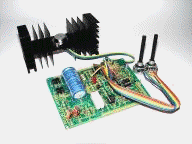
|
How it Works |
|
|
To start with, there is a step-down mains transformer with a secondary winding rated at 24 V/3 A, which is connected across the input points of the circuit at pins 1 & 2. (the quality of the supplies output will be directly proportional to the quality of the transformer). The AC voltage of the transformers secondary winding is rectified by the bridge formed by the four diodes D1-D4. The DC voltage taken across the output of the bridge is smoothed by the filter formed by the reservoir capacitor C1 and the resistor R1. The circuit incorporates some unique features which make it quite different from other power supplies of its class. Instead of using a variable feedback arrangement to control the output voltage, our circuit uses a constant gain amplifier to provide the reference voltage necessary for its stable operation. The reference voltage is generated at the output of U1.
The circuit operates as follows: The diode D8 is a 5.6 V zener, which here operates at its zero temperature coefficient current. The voltage in the output of U1 gradually increases till the diode D8 is turned on. When this happens the circuit stabilises and the Zener reference voltage (5.6 V) appears across the resistor R5. The current which flows through the non inverting input of the op-amp is negligible, therefore the same current flows through R5 and R6, and as the two resistors have the same value the voltage across the two of them in series will be exactly twice the voltage across each one. Thus the voltage present at the output of the op-amp (pin 6 of U1) is 11.2 V, twice the zeners reference voltage. The integrated circuit U2 has a constant amplification factor of approximately 3 X, according to the formula A=(R11+R12)/R11, and raises the 11.2 V reference voltage to approximately 33 V. The trimmer RV1 and the resistor R10 are used for the adjustment of the output voltages limits so that it can be reduced to 0 V, despite any value tolerances of the other components in the circuit.
Schematic diagramm
Another very important feature of the circuit, is the possibility to preset the maximum output current which can be drawn from the p.s.u., effectively converting it from a constant voltage source to a constant current one. To make this possible the circuit detects the voltage drop across a resistor (R7) which is connected in series with the load. The IC responsible for this function of the circuit is U3. The inverting input of U3 is biased at 0 V via R21. At the same time the non inverting input of the same IC can be adjusted to any voltage by means of P2.
Let us assume that for a given output of several volts, P2 is set so that the input of the IC is kept at 1 V. If the load is increased the output voltage will be kept constant by the voltage amplifier section of the circuit and the presence of R7 in series with the output will have a negligible effect because of its low value and because of its location outside the feedback loop of the voltage control circuit. While the load is kept constant and the output voltage is not changed the circuit is stable. If the load is increased so that the voltage drop across R7 is greater than 1 V, IC3 is forced into action and the circuit is shifted into the constant current mode. The output of U3 is coupled to the non inverting input of U2 by D9. U2 is responsible for the voltage control and as U3 is coupled to its input the latter can effectively override its function. What happens is that the voltage across R7 is monitored and is not allowed to increase above the preset value (1 V in our example) by reducing the output voltage of the circuit.
This is in effect a means of maintaining the output current constant and is so accurate that it is possible to preset the current limit to as low as 2 mA. The capacitor C8 is there to increase the stability of the circuit. Q3 is used to drive the LED whenever the current limiter is activated in order to provide a visual indication of the limiters operation. In order to make it possible for U2 to control the output voltage down to 0 V, it is necessary to provide a negative supply rail and this is done by means of the circuit around C2 & C3. The same negative supply is also used for U3. As U1 is working under fixed conditions it can be run from the unregulated positive supply rail and the earth.
The negative supply rail is produced by a simple voltage pump circuit which is stabilised by means of R3 and D7. In order to avoid uncontrolled situations at shut-down there is a protection circuit built around Q1. As soon as the negative supply rail collapses Q1 removes all drive to the output stage. This in effect brings the output voltage to zero as soon as the AC is removed protecting the circuit and the appliances connected to its output. During normal operation Q1 is kept off by means of R14 but when the negative supply rail collapses the transistor is turned on and brings the output of U2 low. The IC has internal protection and can not be damaged because of this effective short circuiting of its output. It is a great advantage in experimental work to be able to kill the output of a power supply without having to wait for the capacitors to discharge and there is also an added protection because the output of many stabilised power supplies tends to rise instantaneously at switch off with disastrous results.

|
Construction |
|
|
First of all let us consider a few basics in building electronic circuits on a printed circuit board. The board is made of a thin insulating material clad with a thin layer of conductive copper that is shaped in such a way as to form the necessary conductors between the various components of the circuit. The use of a properly designed printed circuit board is very desirable as it speeds construction up considerably and reduces the possibility of making errors. To protect the board during storage from oxidation and assure it gets to you in perfect condition the copper is tinned during manufacturing and covered with a special varnish that protects it from getting oxidised and also makes soldering easier.Soldering the components to the board is the only way to build your circuit and from the way you do it depends greatly your success or failure. This work is not very difficult and if you stick to a few rules you should have no problems. The soldering iron that you use must be light and its power should not exceed the 25 Watts. The tip should be fine and must be kept clean at all times. For this purpose come very handy specially made sponges that are kept wet and from time to time you can wipe the hot tip on them to remove all the residues that tend to accumulate on it.
DO NOT file or sandpaper a dirty or worn out tip. If the tip cannot be cleaned, replace it. There are many different types of solder in the market and you should choose a good quality one that contains the necessary flux in its core, to assure a perfect joint every time.
DO NOT use soldering flux apart from that which is already included in your solder. Too much flux can cause many problems and is one of the main causes of circuit malfunction. If nevertheless you have to use extra flux, as it is the case when you have to tin copper wires, clean it very thoroughly after you finish your work.
In order to solder a component correctly you should do the following:
Clean the component leads with a small piece of emery paper.
Bend them at the correct distance from the components body and insert he component in its place on the board.
You may find sometimes a component with heavier gauge leads than usual, that are too thick to enter in the holes of the p.c. board. In this case use a mini drill to enlarge the holes slightly. Do not make the holes too large as this is going to make soldering difficult afterwards.
Take the hot iron and place its tip on the component lead while holding the end of the solder wire at the point where the lead emerges from the board. The iron tip must touch the lead slightly above the p.c. board.
When the solder starts to melt and flow wait till it covers evenly the area around the hole and the flux boils and gets out from underneath the solder.
The whole operation should not take more than 5 seconds. Remove the iron and allow the solder to cool naturally without blowing on it or moving the component. If everything was done properly the surface of the joint must have a bright metallic finish and its edges should be smoothly ended on the component lead and the board track. If the solder looks dull, cracked, or has the shape of a blob then you have made a dry joint and you should remove the solder (with a pump, or a solder wick) and redo it. Take care not to overheat the tracks as it is very easy to lift them from the board and break them.
When you are soldering a sensitive component it is good practice to hold the lead from the component side of the board with a pair of long-nose pliers to divert any heat that could possibly damage the component.
Make sure that you do not use more solder than it is necessary as you are running the risk of short-circuiting adjacent tracks on the board, especially if they are very close together.
When you finish your work, cut off the excess of the component leads and clean the board thoroughly with a suitable solvent to remove all flux residues that may still remain on it.
|
PCB - Connections |
|
|
|
|
pcb.gif (60KB) (12,5cm x 8,7cm)
|
|
| |


|
Construction (... continued) |
|
|
As it is recommended start working by identifying the components and separating them in groups. Place first of all the sockets for the ICs and the pins for the external connections and solder them in their places. Continue with the resistors. Remember to mound R7 at a certain distance from the printed circuit board as it tends to become quite hot, especially when the circuit is supplying heavy currents, and this could possibly damage the board. It is also advisable to mount R1 at a certain distance from the surface of the PCB as well. Continue with the capacitors observing the polarity of the electrolytic and finally solder in place the diodes and the transistors taking care not to overheat them and being at the same time very careful to align them correctly.
Mount the power transistor on the heatsink. To do this follow the diagram and remember to use the mica insulator between the transistor body and the heatsink and the special fibber washers to insulate the screws from the heatsink. Remember to place the soldering tag on one of the screws from the side of the transistor body, this is going to be used as the collector lead of the transistor. Use a little amount of Heat Transfer Compound between the transistor and the heatsink to ensure the maximum transfer of heat between them, and tighten the screws as far as they will go.
Attach a piece of insulated wire to each lead taking care to make very good joints as the current that flows in this part of the circuit is quite heavy, especially between the emitter and the collector of the transistor.
It is convenient to know where you are going to place every thing inside the case that is going to accommodate your power supply, in order to calculate the length of the wires to use between the PCB and the potentiometers, the power transistor and for the input and output connections to the circuit. (It does not really matter if the wires are longer but it makes a much neater project if the wires are trimmed at exactly the length necessary).
Connect the potentiometers, the LED and the power transistor and attach two pairs of leads for the input and output connections. Make sure that you follow the circuit diagram very care fully for these connections as there are 15 external connections to the circuit in total and if you make a mistake it may be very difficult to find it afterwards. It is a good idea to use cables of different colours in order to make trouble shooting easier.
The external connections are:
- 1 & 2 AC input, the secondary of the transformer.
- 3 (+) & 4 (-) DC output.
- 5, 10 & 12 to P1.
- 6, 11 & 13 to P2.
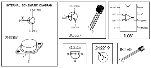
- 7 (E), 8 (B), 9 (E) to the power transistor Q4.
- The LED should also be placed on the front panel of the case where it is always visible but the pins where it is connected at are not numbered.When all the external connections have been finished make a very careful inspection of the board and clean it to remove soldering flux residues. Make sure that there are no bridges that may short circuit adjacent tracks and if everything seems to be all right connect the input of the circuit with the secondary of a suitable mains transformer. Connect a voltmeter across the output of the circuit and the primary of the transformer to the mains.
DO NOT TOUCH ANY PART OF THE CIRCUIT WHILE IT IS UNDER POWER.The voltmeter should measure a voltage between 0 and 30 VDC depending on the setting of P1, and should follow any changes of this setting to indicate that the variable voltage control is working properly. Turning P2 counter-clockwise should turn the LED on, indicating that the current limiter is in operation.
|
Data |
|
|
|
Adjustments |
|
|
If you want the output of your supply to be adjustable between 0 and 30 V you should adjust RV1 to make sure that when P1 is at its minimum setting the output of the supply is exactly 0 V. As it is not possible to measure very small values with a conventional panel meter it is better to use a digital meter for this adjustment, and to set it at a very low scale to increase its sensitivity.
|
Warning |
|
|
While using electrical parts, handle power supply and equipment with great care, following safety standards as described by international specs and regulations.
CAUTION
This circuit works off the mains and there are 220 VAC present in some of its parts.
Voltages above 50 V are DANGEROUS and could even be LETHAL.
In order to avoid accidents that could be fatal to you or members of your family please observe the following rules:
- DO NOT work if you are tired or in a hurry, double check every thing before connecting your circuit to the mains and be ready
- to disconnect it if something looks wrong.
- DO NOT touch any part of the circuit when it is under power.
- DO NOT leave mains leads exposed. All mains leads should be well insulated.
- DO NOT change the fuses with others of higher rating or replace them with wire or aluminium foil.
- DO NOT work with wet hands.
- If you are wearing a chain, necklace or anything that may be hanging and touch an exposed part of the circuit BE CAREFUL.
- ALWAYS use a proper mains lead with the correct plug and earth your circuit properly.
- If the case of your project is made of metal make sure that it is properly earthen.
- If it is possible use a mains transformer with a 1:1 ratio to isolate your circuit from the mains.
- When you are testing a circuit that works off the mains wear shoes with rubber soles, stand on dry non conductive floor
- and keep one hand in your pocket or behind your back.
- If you take all the above precautions you are reducing the
- risks you are taking to a minimum and this way you are protecting
- yourself and those around you.
- A carefully built and well insulated device does not constitute any danger for its user.
- BEWARE: ELECTRICITY CAN KILL IF YOU ARE NOT CAREFUL.
|
If it does not work |
|
|
Check your work for possible dry joints, bridges across adjacent tracks or soldering flux residues that usually cause problems.
Check again all the external connections to and from the circuit to see if there is a mistake there.
- See that there are no components missing or inserted in the wrong places.
- Make sure that all the polarised components have been soldered the right way round. - Make sure the supply has the correct voltage and is connected the right way round to your circuit.
- Check your project for faulty or damaged components.
|
Parts List |
|
|
| R1 = 2,2 KOhm 1W |
| R2 = 82 Ohm 1/4W |
| R3 = 220 Ohm 1/4W |
| R4 = 4,7 KOhm 1/4W |
| R5, R6, R13, R20, R21 = 10 KOhm 1/4W |
| R7 = 0,47 Ohm 5W |
| R8, R11 = 27 KOhm 1/4W |
| R9, R19 = 2,2 KOhm 1/4W |
| R10 = 270 KOhm 1/4W |
| R12, R18 = 56KOhm 1/4W |
| R14 = 1,5 KOhm 1/4W |
| R15, R16 = 1 KOhm 1/4W |
| R17 = 33 Ohm 1/4W |
| R22 = 3,9 KOhm 1/4W |
| RV1 = 100K trimmer |
| P1, P2 = 10KOhm linear pontesiometer |
| C1 = 3300 uF/50V electrolytic |
| C2, C3 = 47uF/50V electrolytic |
| C4 = 100nF polyester |
| C5 = 200nF polyester |
| C6 = 100pF ceramic |
| C7 = 10uF/50V electrolytic |
| C8 = 330pF ceramic |
| C9 = 100pF ceramic |
| D1, D2, D3, D4 = 1N5402,3,4 diode 2A - RAX GI837U |
| D5, D6 = 1N4148 |
| D7, D8 = 5,6V Zener |
| D9, D10 = 1N4148 |
| D11 = 1N4001 diode 1A |
| Q1 = BC548, NPN transistor or BC547 |
| Q2 = 2N2219 NPN transistor |
| Q3 = BC557, PNP transistor or BC327 |
| Q4 = 2N3055 NPN power transistor |
| U1, U2, U3 = TL081, operational amplifier |
| D12 = LED diode |